One reason why the GNSS market is so big is because it keeps getting smaller. Wearables for worker safety and livestock collars for virtual fencing and automated herding are just two examples of how GNSS applications increasingly use compact devices.
But this trend creates a host of challenges for RF and antenna engineers. In a compact GNSS array, isolation between elements is a first-order design parameter. That’s because coupling distorts the array response that the processor depends on and in turn limits how well the array can null. This directly affects the performance and reliability of all the position, navigation, and timing (PNT) applications running on the device.
Isolation also is a top consideration when designing a Controlled Reception Pattern Antenna (CRPA) system to mitigate in-band jamming. This type of spatial filtering uses multiple antenna elements to null out the interfering signals so the receiver can focus on the legitimate GNSS signals. (For a deep dive, see “Inside the Array: How CRPA Systems Mitigate GNSS Jamming.”)
If you’re an RF or antenna engineer laying out a compact, multi-element GNSS board, read on to learn about the four main ways coupling occurs, how to measure it, and the PCB-level techniques for mitigating them and their trade-offs.
A Couple of Problems
Mutual coupling is energy that reaches one element’s port after being received by or radiated from another element. It is reciprocal and measured with S-parameters such as S21.
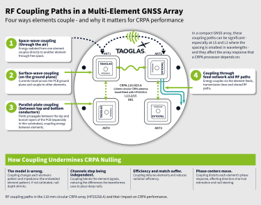
In the case of patch antennas on a shared ground plane, there are four potential routes for coupling to occur:
- Space-wave coupling through the air
- Surface-wave and ground-plane currents
- Parallel-plate modes between the top and bottom conductors
- Coupling through the feed network and RF paths.
Coupling depends on spacing measured in wavelengths, element orientation, ground-plane size, substrate thickness and permittivity, and frequency. It’s typically worst at the lowest band because spacing is smallest in wavelengths at L5 (254.8 mm) and L2.
There are four ways that coupling undermines nulling:
- The model is wrong. The beamformer assumes a known response for each element. Coupling changes every element’s pattern and impedance depending on its neighbors (the “embedded element pattern”). If that is not calibrated, null depth shrinks.
- Channels stop being independent. Weights exploit differences between channels. Coupling blends the channels and reduces those differences.
- Efficiency and match suffer. Coupling detunes elements and reduces radiation efficiency.
- Phase centers move. Coupling distorts each element’s phase response.
PCB-Level Techniques and Their Trade-Offs
There are several PCB-level techniques for mitigating coupling, but each one comes at a cost.
| Technique | How It Works | Trade-Offs |
| More spacing and a larger ground plane | Reduces space-wave and surface-wave coupling. | Larger and heavier board. Spacing above half a wavelength creates grating lobes. |
| Via fences | Rows of plated vias join the top and bottom ground planes between elements and block parallel-plate and surface-wave propagation. | Pitch must be small compared with the guided wavelength (a common rule of thumb is about one tenth; verify). Uses board area. Can shift element tuning. |
| Neutralization network | A deliberate connection between element feeds creates a second coupling path of equal magnitude and opposite phase that cancels the first. | Narrowband and tolerance sensitive. Adds some loss. Harder across L5 to L1, a span of about 29% of the center frequency. |
| Other methods (element orientation, ground-plane slots, shield walls) | Change which modes are excited or block the path. | Complexity and possible effect on polarization purity. |
Implementing isolation solutions directly on the PCB also could restrict the ability to integrate other components or adapt the PCB to a specific application.
To measure coupling:
- Use a four-port vector network analyzer and capture the full S-matrix at L1, L2, and L5. Terminate unused ports in 50 Ω. Report the worst-case pair, not the average.
- Measure embedded element patterns in a chamber, because isolation figures alone do not show how patterns change in the array.
- Follow the application note’s validation list for return loss, isolation, efficiency, gain, radiation patterns and phase-center behavior.
Isolation Targets
−20 dB means 1% of the power couples across, and −30 dB means 0.1%. The right figure depends on the application. Taoglas aims to achieve better than 10 dB isolation.
How to Get Started
Achieving the right isolation in a compact multi-element GNSS array starts with understanding the interactions between the antenna elements, ground plane, PCB layout and RF architecture. Rather than treating isolation as a problem to solve after the board is laid out, consider it early in the design process and validate performance across the required GNSS bands. If you’re working on a compact GNSS or CRPA design, talk to the Taoglas engineering team about your array requirements and how antenna selection, placement and integration can help you achieve the performance your application demands.


